-
E-mail
kemei@cschem.com.cn
-
Phone
0731-82222145
-
Address
3rd Floor, Building C4, Minmetals Technology Industrial Park, No. 28 Lutian Road, Yuelu District, Changsha City
Product Categories
Changsha Kemei Analytical Instrument Co., Ltd
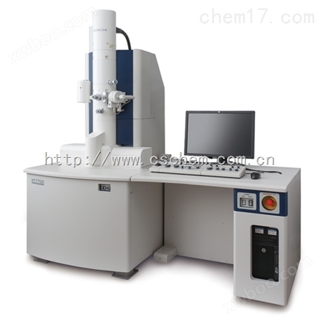
Hitachi in-situ environmental transmission electron microscope H-9500
NegotiableUpdate on 03/18
- Model
- Nature of the Manufacturer
- Producers
- Product Category
- Place of Origin
Overview
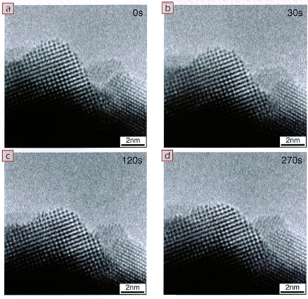
The Hitachi in-situ environmental transmission electron microscope H-9500, with its Z-large feature, can perform real-time in-situ observation. Compared to ordinary transmission electron microscopy, H-9500 can achieve in-situ observation of samples under different conditions (such as gas, heating, etc.) while ensuring high resolution. Similarly, compared to the transmission electron microscope used for in situ observation of sample rods, the H-9500 has a larger sample operation space and no need to worry about damage to the sample rod seal chamber. Its resolution is less affected by the environment and can achieve efficient observation of multiple gases, making it a true in-situ environmental transmission electron microscope.
Product Details
Hitachi in-situ environmental transmission electron microscope H-9500
Product Introduction
H-9500 is a 300kV in-situ environmental transmission electron microscope, which is characterized by its ability to perform real-time in-situ observation. Compared to ordinary transmission electron microscopy, H-9500 can achieve in-situ observation of samples under different conditions (such as gas, heating, etc.) while ensuring high resolution. Similarly, compared to transmission electron microscopy for in-situ observation of sample rods, the sample operation space of H-9500 is larger, and there is no need to worry about damage to the sealed chamber of the sample rod. The resolution is less affected by the environment, and it can achieve efficient operation of multiple gasesObservation of rate is a true in-situ environmental transmission electron microscope.
The main features of Hitachi in-situ environmental transmission electron microscope H-9500 are:
Efficient and fast digital electron microscope
Realize electron beam emission under 300kV high voltage (automatic mode) within 5 minutes, with a sample change time of 1 minute.
Fast and slow dual-mode camera system
Optional electronic direct imaging camera for high-speed in-situ observation
Stable and reliable 5-axis sample stage, low-speed or high-speed sample stage
Sample location memory tracking function
Excellent scalability
FIB expansion fixture, 3D sample rod (optional)
Image database
Easy to operate Windows graphical user interface
Technical Specifications:
| project | Main parameters |
| electron gun | LaB6electron gun |
| accelerating voltage | 300kV、200kV* |
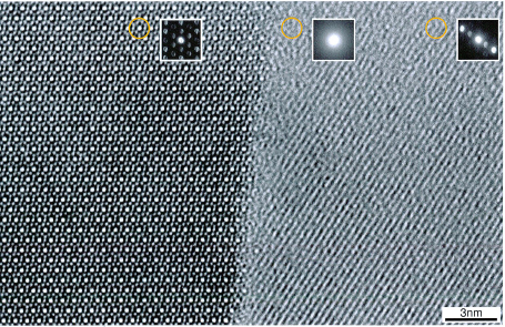
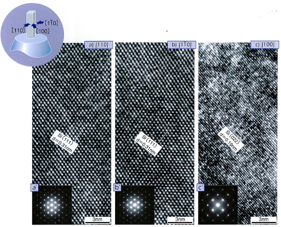
| Point resolution | 0.18nm |
| Line resolution | 0.10nm |
| magnification | Low magnification: 200x -500x |
| Observation: 1000x -1500000x | |
| Electoral District: 4000x -500000x | |
| Illumination system | Lens: Four stage lens; Aperture: 4 holes |
| imaging system | Lens: Five level lens; Objective aperture: 4 holes; Selection aperture: 4 holes |
| sample rod | 5-axis double tilt sample rod, α=β=± 15 ° or greater |
Application fields:
As a true in-situ environmental transmission electron microscope, H-9500 is mainly used for in-situ environmental observation, such as observing various chemical reaction processes, observing the transformation process between different phases of the same material, and real-time observation of the working principle of various nanodevices. Therefore, H-9500 is suitable for multiple fields such as catalysts, fuel cells, nanomaterials and environmental safety, gas sensing components, geochemical materials, etc.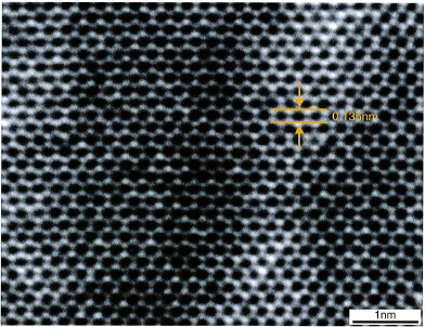
Application article:
[1] Xie1, D. G., Wang1, Z. J., Sun1, J., Li1-3, J., Ma1-4, E., & Shan1, Z. W. In situ study of the initiation of hydrogen bubbles at the aluminium metal/oxide interface. Nature Materials,2015, DOI: 10.1038/NMAT 4336.
[2] Jiang1, Y., Wang1, Y., Zhang2, Y. Y., Zhang1, Z. F., Yuan1, W. T., Sun3, C. H., Wei1, X., Brodsky4, C. N., Tsung4, C. K., Li1, J. X., Zhang5, X. F., Mao6, S. X., Zhang2, S. B. & Zhang1, Z. Direct observation of Pt nanocrystal coalescence induced by electron-excitation-enhanced van der Waals interactions. Nano Research, 2014, 7(3), 308-314.
[3] Peng, H. L., Chan, C. K., Meister, S., Zhang, X. F. & Cui, Y. Shape Evolution of Layer-Structured Bismuth Oxychloride Nanostructures via Low-Temperature Chemical Vapor Transport. Chem. Mater.2009, 21, 247-252.
[4] Vlier1, D. F., Wang1, C., Tripkovic1, D., Strmcnik1, D., Zhang2, X. F., Debe3, M. K., Atanasoski3, R. T., Markovic1, N. M. & Stamenkovic1, V. R. Mesostructured thin films as electrocatalysts with tunable composition and surface morphology. Nature Materials,2012, 11, 1051-1058.
[5] Huo, Z. Y., Tsung, C. K., Huang, W. Y., Zhang, X. F. & Yang, P. D. Sub-Two Nanometer Single Crystal Au Nanowires. Nano Lett. ,2008, 8, 2041-2044.
Similar Product Recommend