-
E-mail
kemei@cschem.com.cn
-
Phone
0731-82222145
-
Address
3rd Floor, Building C4, Minmetals Technology Industrial Park, No. 28 Lutian Road, Yuelu District, Changsha City
Product Categories
Changsha Kemei Analytical Instrument Co., Ltd
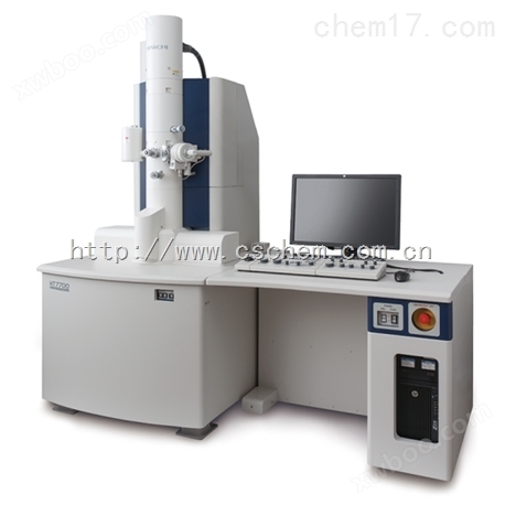
Hitachi aberration corrected scanning transmission electron microscope HD-2700
NegotiableUpdate on 03/18
- Model
- Nature of the Manufacturer
- Producers
- Product Category
- Place of Origin
Overview
Hitachi aberration corrected scanning transmission electron microscope HD-2700 adopts aberration correction technology compared to ordinary transmission electron microscopes, greatly reducing the impact of lens aberration on resolution, thus achieving ultra-high resolution observation. At the same time, HD-2700 is currently one of the few transmission electron microscopes that mainly uses scanning transmission (STEM) function. The large angle gathering STEM function combined with field emission electron gun and aberration correction technology can enable HD-2700 to obtain sub nanometer level electron beams
Product Details
Hitachi aberration corrected scanning transmission electron microscope HD-2700
Product Introduction:
HD-2700 is a 200kV field emission aberration corrected scanning transmission electron microscope. Compared to ordinary transmission electron microscopy, HD-2700 adopts aberration correction technology, greatly reducing the impact of lens aberration on resolution, thus achieving ultra-high resolution observation. At the same time, HD-2700 is currently one of the few transmission electron microscopes that mainly relies on scanning transmission (STEM) functions. The large angle gathering STEM function, combined with field emission electron guns and aberration correction technology, can enable HD-2700 to obtain sub nanometer level electron beams, making atomic level resolution image observation and elemental analysis possible, greatly improving the observation and analysis capabilities of electron microscopes.
The main features of Hitachi aberration corrected scanning transmission electron microscope HD-2700 are:
High-resolution observation
Use gold particles to ensure a standard DF-STEM image with a resolution of 0.144nm.
Large beam analysis
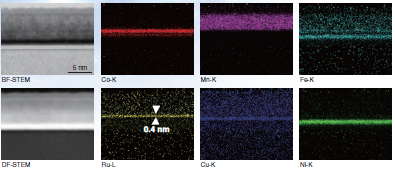
About 10 times the current of a non calibrated STEM probe, it can perform high-speed and high-sensitivity spectral analysis, and obtain the surface distribution map of elements in a shorter time, making it possible to detect trace elements.
Simplified operation
The provided GUI automatically adjusts the spherical aberration corrector
Overall solution
The sample rod is compatible with Hitachi FIB and provides a comprehensive solution at the nanoscale, from sample preparation to data acquisition and final analysis
Multiple evaluation and analysis functions to choose from
Can simultaneously obtain and display SE&BF, SE&DF, BF&DF, DF/EDX, and DF/EELS images; Can be equipped with ELV-2000 real-time element mapping system (DF-STEM images can be obtained simultaneously); It is possible to observe both DF-STEM images and diffraction images simultaneously; It can be equipped with ultrafine column head sample rods for three-dimensional analysis (360 degree rotation), etc.
Technical Specifications:
| project | Main parameters |
| electron gun | Cold or hot field emission electron gun |
| accelerating voltage | 200kV、120kV* |
| 0.144nm (standard type, equipped with aberration, cold or hot field) | |
| Line resolution | 0.136nm (high-resolution type, equipped with aberration and cold field) |
| 0.204nm (standard type, equipped with thermal field, no spherical aberration) | |
| magnification | 200x - 10,000,000x |
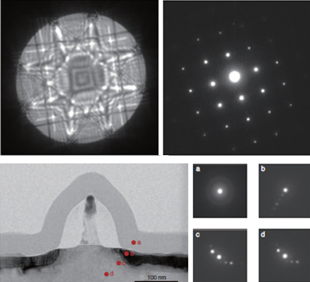
| Image mode | BF-STEM phase contrast image (TE image), DF-STEM atomic number contrast image (ZC image), secondary electron image (SE image), electron diffraction pattern (optional), characteristic X-ray image (optional: EDX), EELS image (optional: ELV-2000) |
| Electron optics | Electron gun: cold or hot field emission electron gun with built-in anode heater |
| Lens system: two-stage condenser, objective lens, projection lens | |
| Ball aberration corrector: hexapole/transmission dual (standard and high-resolution) | |
| Scanning coil: two-stage electromagnetic coil | |
| Potential shift: ± 1 μ m | |
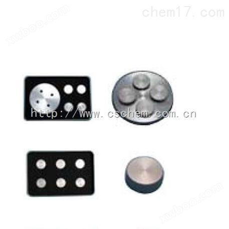
| sample rod | Side insertion type, X=Y=± 1mm, Z=± 0.4mm, T=± 30 ° (single tilt sample rod) |
Application areas:
HD-2700, as a field emission spherical aberration correction scanning transmission electron microscope, not only has high-resolution image observation ability, but also has high spatial resolution analysis ability. Combined with EELS and EDS, it can achieve atomic level element analysis. HD-2700 has multiple imaging modes that can meet the observation needs of most samples. Hitachi's SE imaging mode can obtain surface information of samples that transmission electron microscopy cannot obtain, while also having higher resolution than ordinary scanning electron microscopy, enabling high-resolution observation of sample surfaces.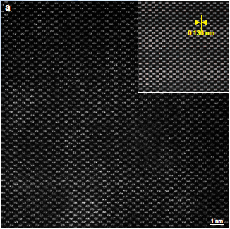
Application article:
[1] Ciston1, J., Brown2, H. G., D`Alfonso2, A. J., Koirala3, P., Ophus1, C., Lin3, Y., Suzuki4, Y., Inada5, H., Zhu6, Y. & Marks3, L. D. Surface determination through atomically resolved secondary electron imaging. Nature Communications,2005,6, 7358-7365.
[2] Zhu1*, Y., Inada2, H., Nakamura2, K. & Wall1, J. Imaging single atoms using secondary electrons with an aberration-corrected electron microscope. Nature Materials,2009,8, 808-812.
Similar Product Recommend